
Set – 1 (15th February 2014 (Forenoon))
1.
In the figure, assume that the forward voltage
drops to the PN diode D1 and Schottky diode D2 are 0.7
volts and 0.3 volts respectively. If ON denotes conducting state of the diode
and OFF denotes the non conducting state of the diode, then in the circuit,

a.
Both are ON
b.
D1 is ON and D2 is OFF
c.
Both are OFF
d.
D1 is OFF and D2 is ON
Solution : https://www.youtube.com/watch?v=qteoesfhVco
2.
A good current buffer has
a.
Low input impedance and low output impedance
b.
Low input impedance and high output impedance
c.
high input impedance and low output impedance
d.
high input impedance and high output impedance
Solution : https://www.youtube.com/watch?v=vdYmByP9zYY
3.
In the ac equivalent circuit shown in the
figure, if iin is the input current and RF is very large,
then the type of feedback is

a.
Voltage – Voltage feedback
b.
Voltage – Current feedback
c.
Current – Voltage feedback
d.
Current – Current feedback
Solution : https://www.youtube.com/watch?v=otvYW4oudRg
4.
In the low pass filter shown in the figure, for
a cutoff frequency of 5 KHz, the value of R2 (in KΩ)
is ……..

Solution : https://www.youtube.com/watch?v=BjcHUWQA4TQ
5.
A BJT is biased in forward active mode. Assume VBE
= 0.7 volts, KT/q = 25 mV and reverse saturation current IS = 10-13
Amp. The Transconductance of the BJT (in mA/volt) is…..
Solution : https://www.youtube.com/watch?v=nAh0aTdVp84
6.
In the voltage regulator circuit shown in the
figure, the Op-Amp is ideal. The BJT has VBE = 0.7 volts, and β =
100, and the zener voltage is 4.7 volts. For a regulated output of 9 volts, the
value of R (in Ω) is ……..

Solution : https://www.youtube.com/watch?v=B5rropdO8jA
7.
In the circuit shown, the Op-Amp has finite
input resistance, infinite voltage gain and zero input offset voltage. The
output voltage Vout is …….

a.
– I2(R1 + R2)
b.
I2R2
c.
I1R2
d.
– I1(R1 + R2)
Solution : https://www.youtube.com/watch?v=DAEuj8Z-ncY
8.
For the amplifier shown in the figure, the BJT
parameters are VBE = 0.7 volts, β = 200, and thermal voltage VT
= 25 mV. The voltage gain (vo/vi) of the amplifier is
……..

Solution : https://www.youtube.com/watch?v=YTAqzayIguA
SET – 2 (15th February 2014 (Afternoon))
1.
The diode in the circuit shown, if Von
= 0.7 volts but is ideal otherwise. If Vi = 5 sin(ωt)
volts, the minimum and maximum values of Vo (in volts) are,
respectively,

a.
-5 and 2.7
b.
2.7 and 5
c.
-5 and 3.85
d.
1.3 and 5
Solution : https://www.youtube.com/watch?v=VNI1bsbW2i8
2.
The feedback topology in the amplifier circuit
(the base bias circuit is not shown for simplicity) in the figure is
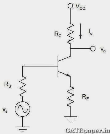
a.
Voltage – Shunt feedback
b.
Current – Series feedback
c.
Current – Shunt feedback
d.
Voltage – Series feedback
Solution : https://www.youtube.com/watch?v=MNduRhMC6zk
3.
In the differential amplifier shown in the
figure, the magnitude of the common mode and differential mode gains are Acm
and Ad, respectively. If the resistance RE is increased,
then

a.
Acm increases
b.
Common mode rejection ratio increases
c.
Ad increases
d.
Common mode rejection ratio decreases
Solution : https://www.youtube.com/watch?v=AhxODnKBU5Y
4.
A cascade connection of two voltage amplifiers
A1 and A2 is shown in the figure. The open loop gain Avo, input
resistance Rin, and output resistance Ro for A1 and A2
are as follows:
A1 : Avo = 10, Rin = 10 KΩ, Ro = 1 KΩ
A2
: Avo = 5, Rin = 5 KΩ, Ro = 200 Ω
The approximate overall voltage gain Vout
/ Vin is …………….

Solution : https://www.youtube.com/watch?v=ijiC9w_XNuw
SET – 3 (16th February 2014 (Forenoon))
1.
In the circuit shown, the PNP transistor has |VBE|
= 0.7 volts and β = 50. Assume that RB = 100 KΩ.
For Vo to be 5 volts, the value of RC (in KΩ)
is ……..

Solution : https://www.youtube.com/watch?v=ohf5m4r0gzs
2.
The desirable characteristics of a
Transconductance amplifier are
a.
High input resistance and High output resistance
b.
High input resistance and Low output resistance
c.
Low input resistance and High output resistance
d.
Low input resistance and Low output resistance
Solution : https://www.youtube.com/watch?v=1RsZ43lyRhs
3.
The figure shows a half wave rectifier. The
diode D is ideal. The average steady state current (in Amperes) through the
diode is approximately…………

Solution : https://www.youtube.com/watch?v=vubUa_xDnIk
4.
Assuming that the Op-Amp in the circuit is ideal, then the output voltage is

Solution : https://www.youtube.com/watch?v=Q7DUP4Rz58o
5.
In the circuit shown, the silicon BJT has β =
50. Assume VBE = 0.7 volts and VCEsat = 0.2 volts. Which
one of the following statements is correct?

a.
For RC = 1 kΩ, the BJT operates in the saturation
region
b.
For RC = 3 kΩ, the BJT operates in the saturation
region
c.
For RC = 20 kΩ, the BJT operates in the cutoff
region
d.
For RC = 20 kΩ, the BJT operates in the linear
region
Solution : https://www.youtube.com/watch?v=zd_NFD2CN8E
SET
- 4 (16th February 2014 (Afternoon))
1.
If the emitter resistance in a common emitter
voltage amplifier is not bypassed, it will
a.
Reduce both the voltage gain and the input
impedance
b.
Reduce the voltage gain and increase the input
impedance
c.
Increase the voltage gain and reduce the input impedance
d.
Increase both the voltage gain and the input
impedance
Solution : https://www.youtube.com/watch?v=4YjclPDw5lM
2.
Consider two BJTs biased at the same collector
current with area A1 = 0.2 µm x 0.2 µm and A2 = 300 µm
x 300 µm.
assuming that all other device parameters are identical, KT/q = 26 mV, the
intrinsic carrier concentration is 1 x 1010 cm-3, and q =
1.6 x 10⁻¹⁹C, the difference between the base emitter voltages (in
mV) of the two BJTs (i.e. VBE1 – VBE2) is …………….
Solution : https://www.youtube.com/watch?v=R-GogUWvN74
3.
A BJT in a common base configuration is used to
amplify a signal received by a 50Ω antenna. Assume KT/q = 25 mV, the
value of collector bias current (in mA) required to match the input impedance
of the amplifier to the impedance of the antenna is ………..
Solution : https://www.youtube.com/watch?v=HBjqJb91WbE
4.
Two silicon diodes, with a forward voltage drop
of 0.7 volts, are used in the circuit shown in the figure. The range of input
voltage Vi for which the output voltage Vo = Vi, is

a.
-0.3 volts < Vi < 1.3 volts
b.
-0.3 volts < Vi < 2 volts
c.
-1.0 volts < Vi < 2.0 volts
d.
-1.7 volts < Vi < 2.7 volts
Solution : https://www.youtube.com/watch?v=6GsjQs9DKbU
5.
The circuit represents

a.
A band pass filter
b.
A voltage controlled oscillator
c.
An Amplitude modulator
d.
A monostable multivibrator
Solution : https://www.youtube.com/watch?v=oi_nPP2yd4k
6.
Consider the common collector amplifier in the
figure (bias circuitry ensures that the transistor operates in forward active
region, but has been omitted for simplicity). Let IC be the collector
current, VBE be the base emitter voltage and VT be the
thermal voltage. Also, gm and ro are the small signal Transconductance
and output resistance of the transistor, respectively. Which one of the
following conditions ensures a nearly constant small signal voltage gain for a
wide range of values of RE?

Solution : https://www.youtube.com/watch?v=Xur5bWVoR10
7.
For the common collector amplifier shown in the
figure, the
BJT has high β, negligible VCEsat and VBE
= 0.7 volts. The maximum undistorted peak to peak output voltage Vo
(in volts) is ………

Solution : https://www.youtube.com/watch?v=LsXNjgHVeK0
No comments:
Post a Comment