
Video Lecture Series from IIT Professors :
Electronic Devices by Prof. A.N. Chandorkar sir

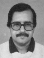
Dr. A.N. Chandorkar
Academic Background
- Ph.D. degree in Electrical Engineering, January 1978,University of Rajasthan, Jaipur. Thesis:’Influence of Schottky Barrier Injection on negative resistance Microwave Semiconductor Diode’.
- Research Work carried at CEERI, Pilani, Rajasthan. Research Supervisor: Dr. W.S.Khokle, Former Director, CEERI, Pilani.
- Master of Science Technology, in Electronics Engineering, 1969. Thesis:’Study of TTL Logic Circuits’, Supervisor: Prof. K.V. Ramanathan
Research Interests
- Analog and Mixed signal VLSI Design
- Ultra-Thin Gate insulators for VLSI Technologies
- High-K Dielectrics for VLSI Technologies (Nano Electronics)
- RF VLSI Design
- Radiation Hard MOS Technologies
- Communication/DSP based System and chip Design
- Semiconductor Device modelling and Reliability Simulation Tools
- Memory Testing, Analog and Mixed signal Test and Fault simulation
- Accelerated Device Testing and Reliability,
- Modelling,High Power semiconductor Devices, Power Electronic Systems, Optically Switched Microwave components, Sensors
- Microelectronics System Packaging
Contact Information
Department of Electrical Engineering
IIT Bombay, Powai
Mumbai 400 076, India
Email : anc[AT]ee.iitb.ac.in
Phone (Internal(O)) : (0091 22) - 2576 7441
Phone (Internal(R)) : 8441
Office room no: EE 132
Fax: (0091 22) - 25723707
IIT Bombay, Powai
Mumbai 400 076, India
Email : anc[AT]ee.iitb.ac.in
Phone (Internal(O)) : (0091 22) - 2576 7441
Phone (Internal(R)) : 8441
Office room no: EE 132
Fax: (0091 22) - 25723707
